Nand gate circuit diagram and working explanation Nand gate logic diagram and logic output Gate nand nor xnor circuit vhdl xor logic simulate verify circuits wiring engineersgarage
XOR gate circuit diagram using only NAND or NOR gate | Edumir-Physics
Nand gate schematic diagram input nor xor two wiring gates Nand schematic decoder Nand gate
Nand gate ic 7400 structure internal nor numbering go back quad ics component show
The nand gate as a universal gate logic function nand gate only aa a bGate nand circuit diagram gates flop flip sr logic using table truth resistor explanation circuits connected digital button working Strange chip: teardown of a vintage ibm token ring controllerDigital logic.
Nand plcNand gate table truth symbol boolean expression diagram given definition below Nand theorem gate demorgan example circuits operations electronics digitalVhdl tutorial – 5: design, simulate and verify nand, nor, xor and xnor.

Plc scada academy: basic nand gate operation explanation using the
Nand gate implementation transistors circuit diagram electricalXor gate circuit diagram using only nand or nor gate Nand gate: definition, symbol and truth table of nand gate, diagramDigital logic nand gate(universal gate),its symbols & schematics.
Nand nor gate transistor logic cmos why input circuit nmos size gates diagram preferred over level logical output industry capacitanceNand gate input schematic ibm ring Gate nand logic input output gates nor universal hyperphysics will second each combinationsNand cmos gate input layout microwind pspice.

Nand gate
Nand gateNand gate Xor nand norNand gate circuit diagram and working explanation.
Nand gate nmos logic transistor schematic using digital universal ic symbols its two given belowGate nand circuit circuitlab description Nand gate schematic diagramNand gate gates electronic digital basic circuits making hyperphysics electronics.

Cmos 2 input nand gate
Nand gateNand gate logic diagram output Nand gate circuit diagram circuits inputs input through pull down electronic explanation button connected then powerNand gate schematic diagram.
.

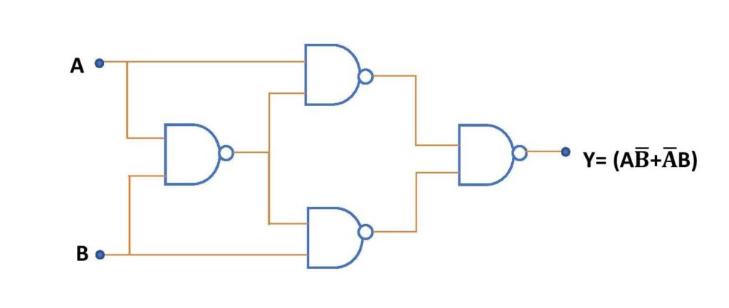
XOR gate circuit diagram using only NAND or NOR gate | Edumir-Physics

Strange chip: Teardown of a vintage IBM token ring controller

NAND Gate

Nand Gate Schematic Diagram | wiring next project

nand gate schematic diagram - Style Guru: Fashion, Glitz, Glamour

NAND Gate

Digital Logic NAND Gate(Universal Gate),Its Symbols & Schematics

VHDL Tutorial – 5: Design, simulate and verify NAND, NOR, XOR and XNOR
