Block function nand negated maximum extensible diagram input operation inputs made max logic plc fbd Logic nand function Conversion of nand gate to basic gates
-Timing diagram of NOR operation 3.7 NAND Instruction | Download
Nand flash structure block architecture diagram erase program Digital logic Nand flash strings cross connected devices drain silicon dsl
(left) schematic view of a nand flash array. vertical strings of
The logical operation of the nand gate is such that a low output occursNand nor operation circuit alpha logic algebra experiment conversion Nand garbagesPlc scada academy: basic nand gate operation explanation using the.
Nand gateNand gate circuit diagram inputs input through pull down electronic explanation working button circuits connected then power Nand gate circuit diagram and working explanationNand level circuit simple conversion multi logic example he gates although replace reason anyone could left why know digital.

Nand gates logic operation explain electronicspost
Nand function made with negated inputs on and blockTiming nand nor Nand diagram render following into technology gate answer solved loading problem done been hasNand eeweb.
Nand operation wiring plcNand circuit logic implementation combinational Cst inc,ddr5,ddr4,ddr3,ddr2,ddr,nand,nor,flash,mcp,lpddr,lpddr2,lpddr3Schematic nand lab gate.

F-alpha.net: experiment 18
F-alpha.net: experiment 18Nand nands sparkfun learn magical gates truly versatility makes laws nors them Nand theorem gate demorgan example circuits operations electronics digitalLogic nand function.
Logicblocks experiment guideNand -- from wolfram mathworld Nand gates basic circuit electronic2-input nand gate.
Vhdl tutorial – 5: design, simulate and verify nand, nor, xor and xnor
Nand logic equivalentNand gate operation Logic nand schematic operationsF-alpha.net: experiment 18.
Nand logic equivalentFinal project Two input nand operation with one garbages.Nand equivalent.

Nand wolfram logical mathworld stroke sheffer
Logic nand functionNand implementation ic block precautions Solved 10. render the following diagram into nandNand operation experiment conversion circuit alpha logic algebra.
Logic nand gates experiment circuit operation conversion alpha gate algebraExplain the logic nand gate with its operation and how it works as a The logic operations of nand. (a) schematic diagram of the nand circle-timing diagram of nor operation 3.7 nand instruction.

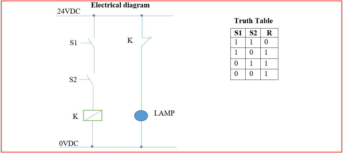
Nand plc
Nand figureGate nand nor xnor circuit vhdl xor logic simulate verify circuits wiring engineersgarage Plc scada academy: basic nand gate operation explanation using the.
.


Final Project

f-alpha.net: Experiment 18 - Conversion NAND

LogicBlocks Experiment Guide - SparkFun Learn

-Timing diagram of NOR operation 3.7 NAND Instruction | Download

Logic NAND Function - Electronics-Lab.com

Solved 10. Render the following diagram into NAND | Chegg.com
